

SiCウエハー
SiC wafer
SiCウエハー
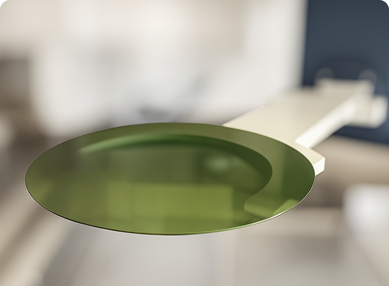
SiCウエハー(炭化ケイ素ウエハー)は、シリコン(Si)と炭素(C)からなる化合物半導体「SiC(Silicon Carbide)」を基材としたウエハーです。従来のシリコンウエハーに比べて、絶縁破壊電界が高く、高電圧環境でも安定して動作するほか、熱伝導性にも優れており、発熱を効率よく逃がすことができます。これにより冷却設計が簡素化され、装置の小型化にも貢献します。また、スイッチング損失が小さく、高周波領域でも高効率な電力変換が可能となるため、電気自動車(EV)や再生可能エネルギー関連機器、通信インフラ、産業用電源装置など、幅広い分野での応用が進んでいます。
SiCウエハー
— 極限環境に挑む革新素材 —
SiCウエハー(炭化ケイ素ウエハー)、高温・高耐圧・高周波といった過酷な条件下でも安定動作を可能にする、次世代の半導体基板です。
トリニティーでは、SiCウエハーを中心に、パワーデバイスやEVインバーター、急速充電器、産業用モーター制御などの用途に対応した高品質素材を提供しています。
高硬度・高熱伝導性・広いバンドギャップを備えたSiCは、電力損失の低減や装置の小型・軽量化に貢献し、再生可能エネルギーや電動化の加速に不可欠な技術基盤となっています。
さらに、試作から量産までの加工・検査・納品を一貫して支援する体制により、開発スピードと品質の両立を実現。
トリニティーは、SiCの可能性を最大限に引き出す素材選定と供給を通じて、持続可能な未来のものづくりを支えます。
導入用途・販売実績

次世代電動化・高周波分野で拡大するSiC導入実績と応用展開
トリニティーのSiCウエハーおよびインゴットは、EVインバーター、急速充電器、太陽光パワコン、産業用モーター制御、5G基地局など、電力効率と高周波性能が求められる先端分野で多数導入されています。
国内外のパワーデバイスメーカーや研究機関との取引実績を通じて、4インチ・6インチ・8インチ対応の高品質SiC素材を安定供給し、試作から量産までの技術支援を一貫して提供。
高耐圧・高温・高周波環境下での動作を可能にするSiCは、次世代電動化・再生可能エネルギー・通信分野のキーマテリアルとして、採用が急速に拡大しています。
トリニティーは、用途に応じた素材選定と柔軟な供給体制を通じて、SiCの可能性を最大限に引き出し、未来のものづくりを支えます。
トリニティーでは、エピ成長に適した低欠陥・高均質なSiCウエハーを提供。表面処理、結晶方位、抵抗値などの仕様調整に加え、エピ工程での歩留まり向上や膜厚均一性の評価支援も実施。国内外のエピメーカーとの連携実績を活かし、開発スピードと品質の両立を支援します。
他の製品を見る


お問い合わせ
製品に関するご相談、加工・検査のご依頼、資料請求、その他ご質問など、
どんなことでもお気軽にお問い合わせください。
専門スタッフが内容を確認のうえ、迅速かつ丁寧に対応させていただきます。
ご希望の仕様や納期、ご予算に関するご相談も承っております。
試作から量産まで、お客様のニーズに合わせた最適なご提案をいたします。
お急ぎの方はお電話にてお問い合わせください。